8T49N281 Universal Frequency Translator
8T49N281 Universal Frequency Translator
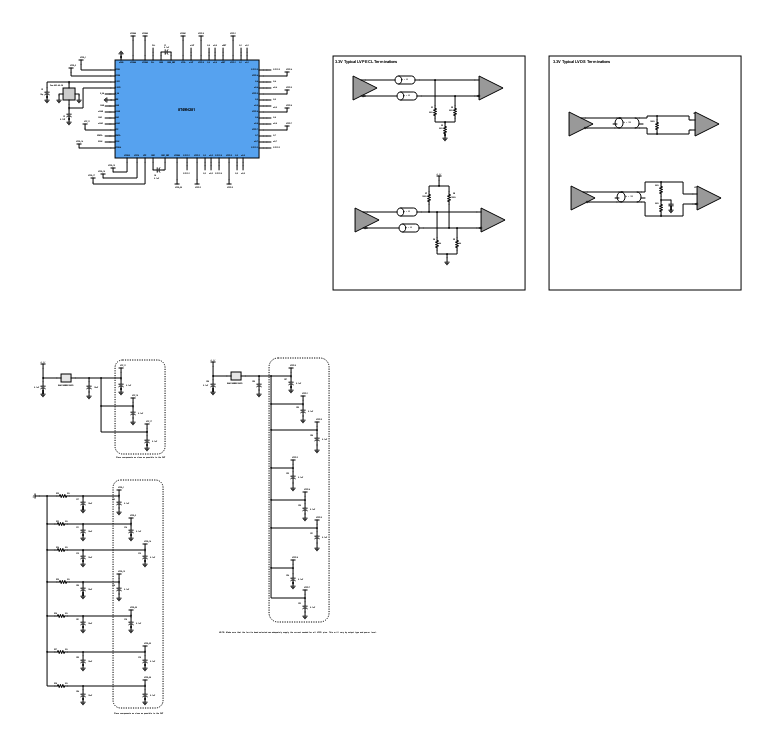
The 8T49N281 accepts up to two differential or single-ended input clocks and a crystal input. The PLL can lock to either input clock, but both input clocks must be related in frequency. The device supports hitless reference switching between input clocks. The device monitors both input clocks for Loss of Signal (LOS). It generates an alarm when an input clock failure is detected. The automatic and manual hitless reference switching options are supported. The LOS behavior can be set to support gapped or un-gapped clocks. In the circuit, the clock layout topology is a typical termination for LVPECL outputs. The differential outputs generate ECL/LVPECL compatible outputs. Therefore, terminating resistors (DC current path to ground) or current sources must be used for functionality. These outputs are designed to drive 50Ω transmission lines. The matched impedance techniques should be used to maximize operating frequency and minimize signal distortion. The values of the resistors can be increased to reduce the loading for slower and weaker LVCMOS driver. When using single-ended signaling, the noise rejection benefits of differential signaling are reduced. Even though the differential input can handle full rail LVCMOS signaling, it is recommended that the amplitude be reduced. A typical point-to-point LVDS design uses a 100Ω parallel resistor at the receiver and a 100Ω differential transmission-line environment. In order to avoid any transmission-line reflection issues, the components should be surface mounted and must be placed as close to the receiver as possible. IDT offers a full line of LVDS compliant devices with two types of output structures: current source and voltage source.
The frequency translation has various applications which can be used in data communications, wireless base station baseband, OTN de-mapping (Gapped Clock and DCO mode) and OTN or SONET / SDH equipment Line cards (up to OC-192, and supporting FEC ratios). In addition, the device may also behave as a frequency synthesizer.
Read more
Incorporated Products
IMAGE
MANUFACTURER PART NUMBER
DESCRIPTION
QUANTITY
VIEW DETAILS

.jpg)
You are about to delete project
Please type 'DELETE' (without quotes) to the below box to confirm the deletion: