Scheme-it
Introduction
Schematic Drawings

Use schematic symbols to layout the components of your circuit and make electrical connections. With symbols ranging from amplifiers to vacuum tubes, as well as the ability to build custom symbols, you are able to design nearly any circuit. Access to Digi-Key's extensive part database also allows you to browse and assign orderable part numbers.
Diagram Building
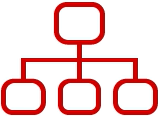
Use the system blocks to refine your idea at a conceptual level. The higher-level components are there to help you plan out the broader intentions of your idea. This powerful block chain library allows you to quickly layout the function of circuit. Once your design is ready, save and share with your colleagues.
Flow Chart Creation
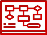
The flow chart creation option will help transition your concept to a design. Use the library of arrows, shapes, UML symbols, and more to sort out the flow and annotate each stage. Insert a textbox, math function/formula, image, or link to help illustrate the objectives and make your plan easy to follow.
Projects
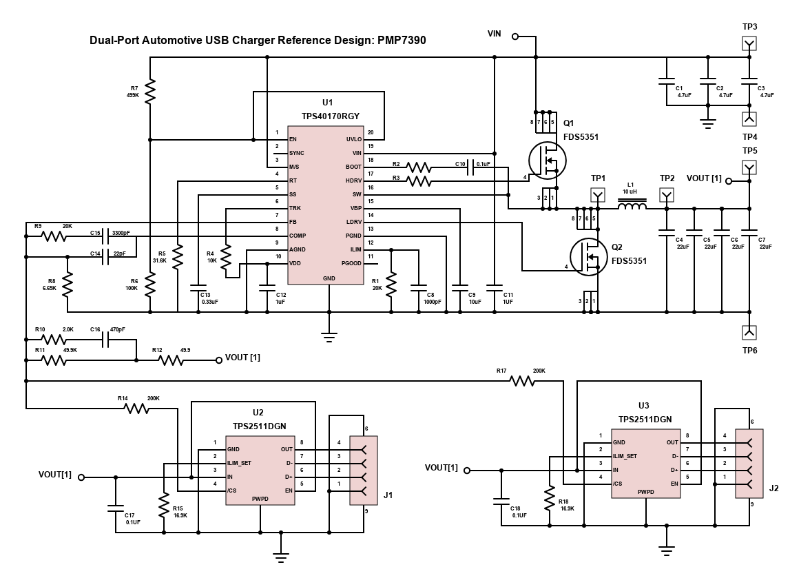
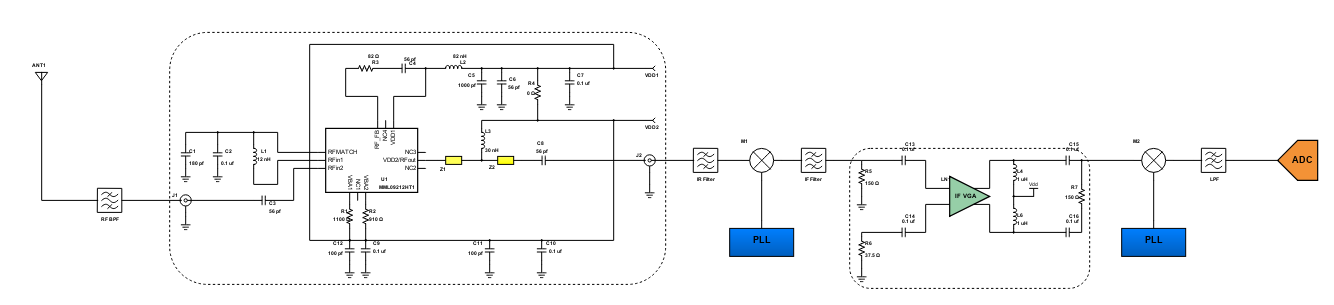
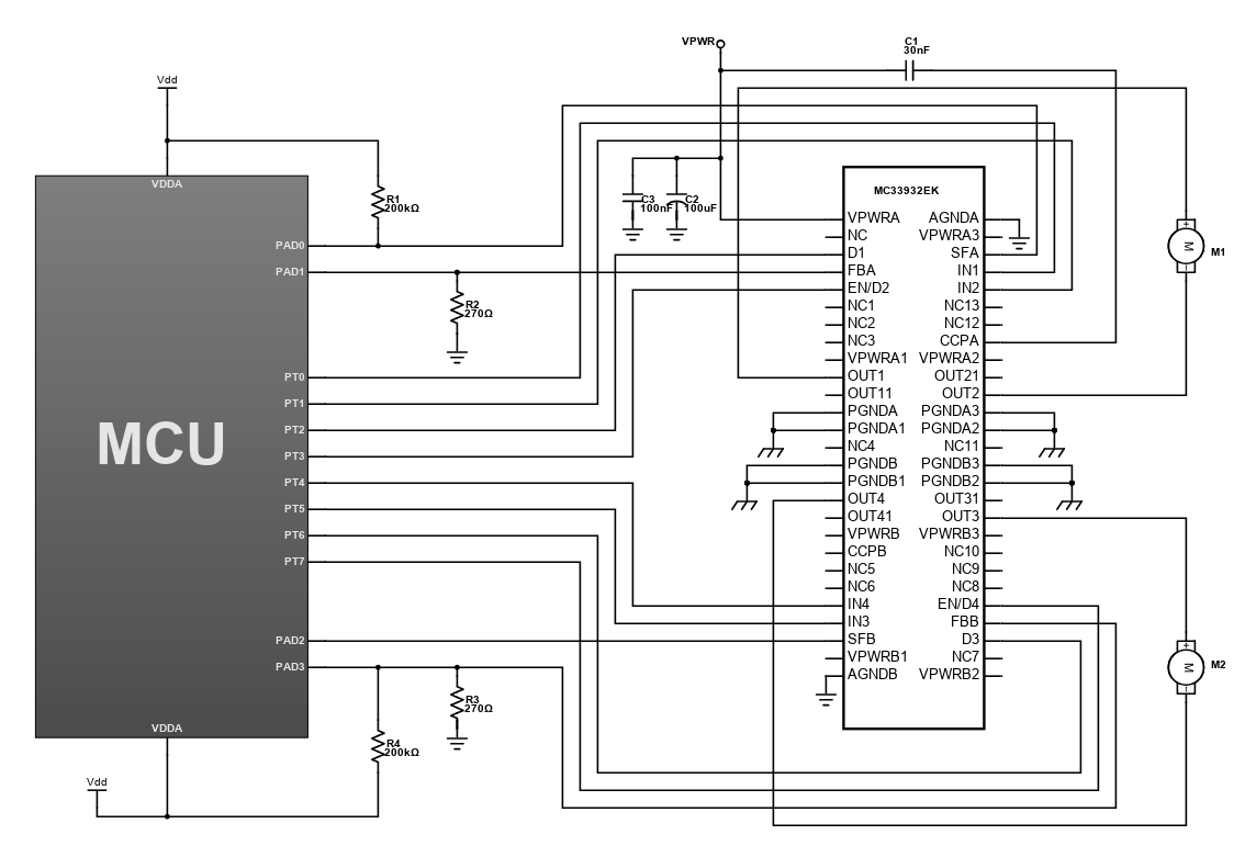
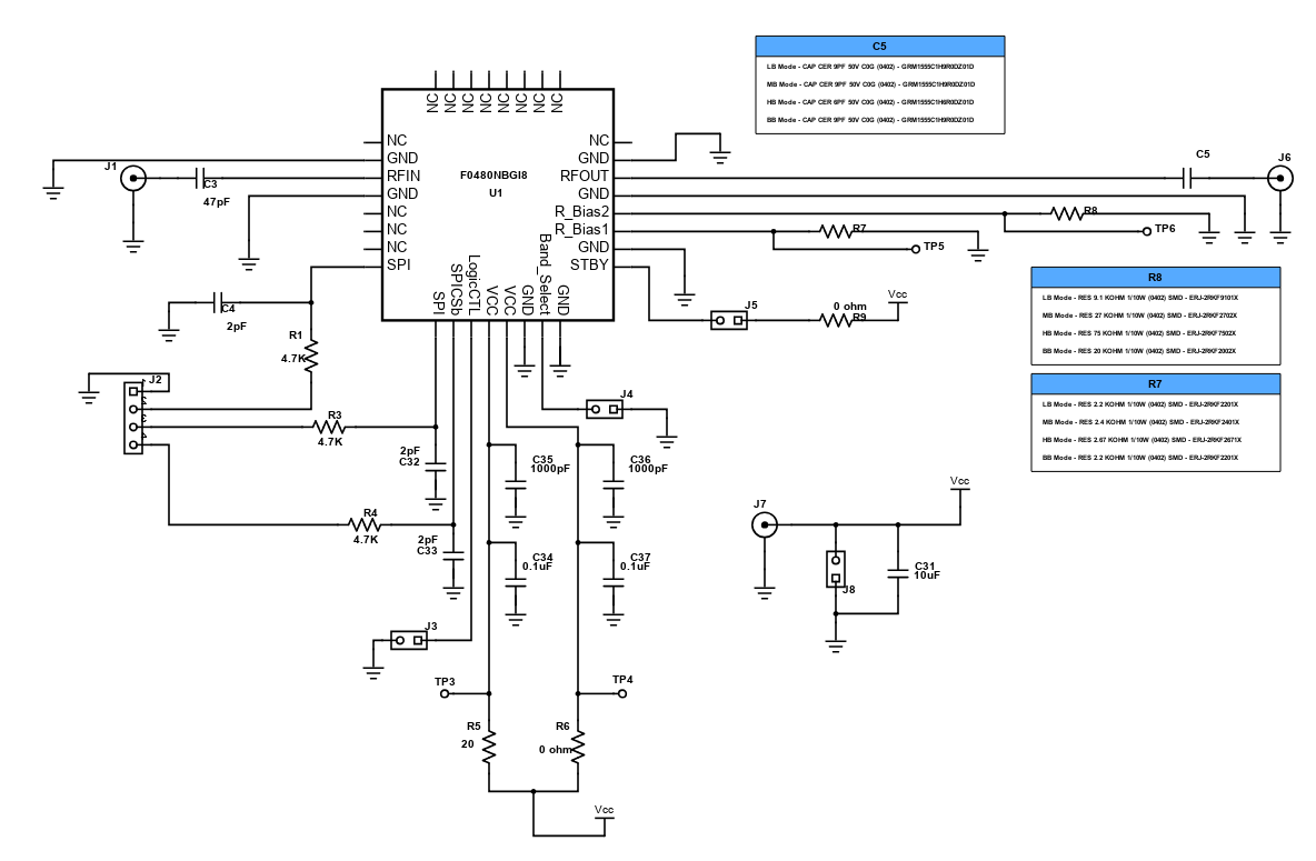
Design Starters help give you a running start for your next design. Whether you are looking to begin a wireless charging platform or quickly design around a Bluetooth Low Energy module, our Design Starters will help get you quickly on your way.
Digi-Key has worked with industry leaders to help drive almost instantaneous ideation and these starters are ideal building blocks to help get your concepts created, drawn and documented in almost no time at all. Featured Design Starters
12 items
Refine Search
APPLICATION
MANUFACTURER
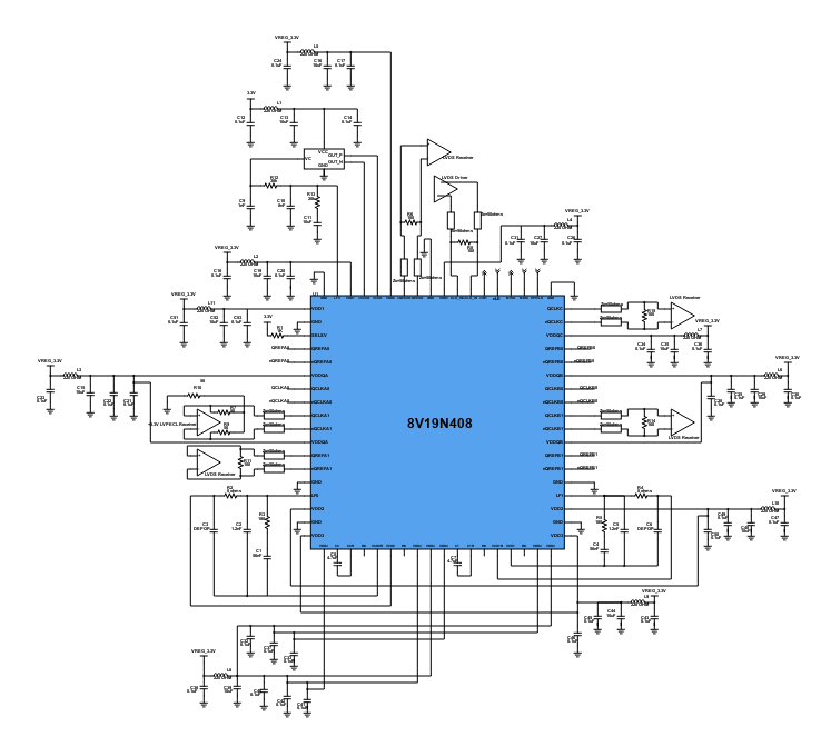
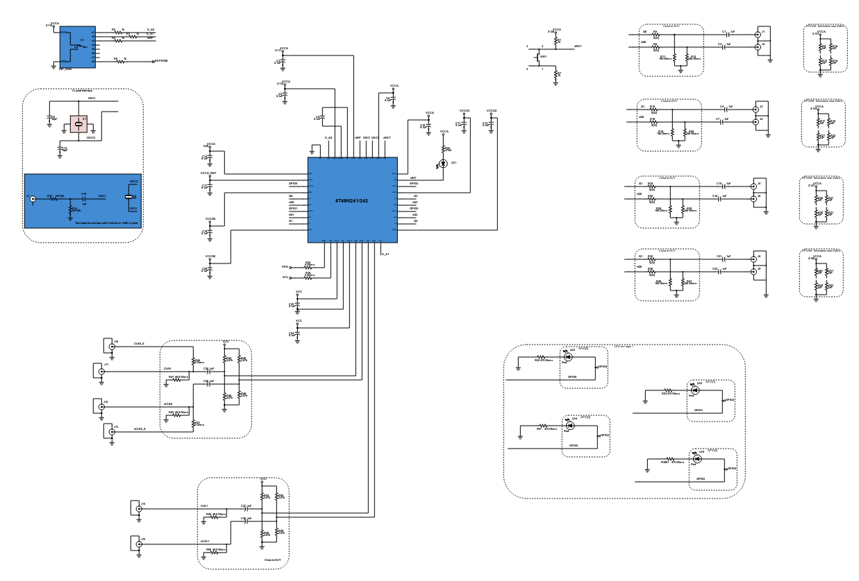
8T49N241/242 FemtoClock NG Universal Frequency Translator with fractional output dividers
The demand of reliable Information Technology (IT) equipment like IP switches/routers brought out another challenge to embedded developers. In this case, the increase of the size of data transfers through electronic communication system requires equipment that could handle the operation properly. This design of universal frequency translators features a femtoclock UFT IC that has a one fractional-feedback PLL. It can be used as a frequency synthesizer or a frequency translator with jitter attenuation. It offers four independent programmable clocking outputs with up to three fractional output dividers. It supports SONET/SDH clocks including FEC rate conversions and accepts LVPECL, LVDS, LVHSTL, HCSL or LVCMOS input clocks.
8T49N004 Programmable Femtoclock® NG with 4-outputs
This design features a fourth generation programmable femtoclock that provides reference frequencies to replace crystals and SAW oscillators in high-performance applications. It is programmable through I2C interface. It has four selectable LVPECL or LVDS via I2C while its FemtoClock NG VCO ranges between 1.9GHz to 2.55GHz. It also meets the standard interface requirements of PCI Express (2.5Gb/s), Gen 2 (5Gb/s), and Gen 3 (8Gb/s) jitter that are low in both clock synthesizers and phase-locked oscillators.
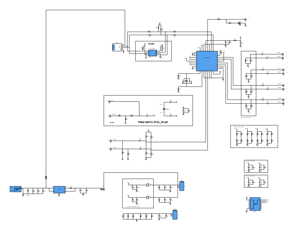
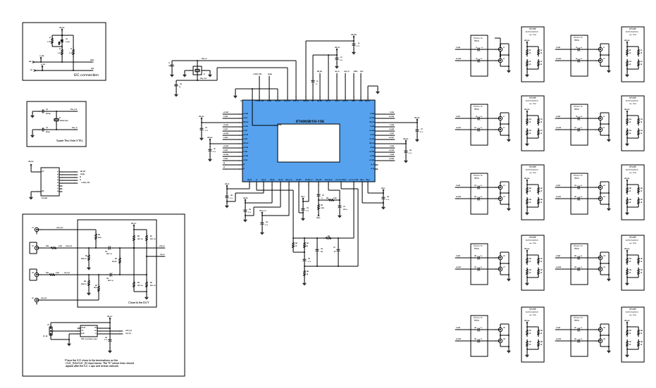
8T49NS010 Clock Synthesizer and Fanout Buffer/Divider
This reference design features the 8T49NS010 integrated circuit that functions as a clock synthesizer with a built-in fanout buffer and divider. By using an external clock source or a crystal, the 8T49NS010 can generate high performance timing geared towards the communications and datacom markets, especially for applications demanding extremely low phase noise jitter, such as 10, 40 and 100GE. Depending on the input used, the 8T49NS010's low phase noise integer-N PLL can multiply the reference to 2400MHz or 2500MHz.
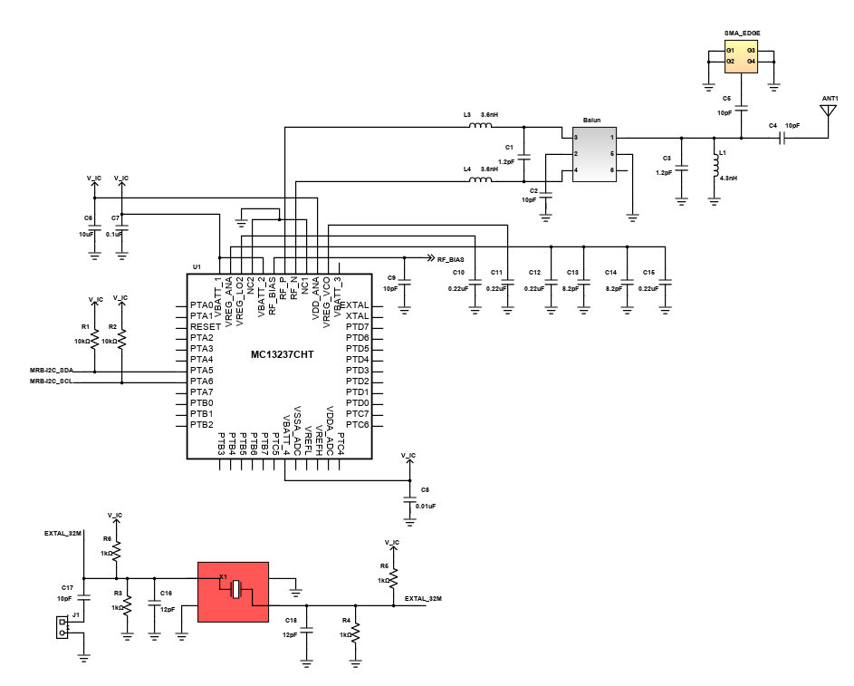
8T49N028 Low RMS Phase Jitter Clock Synthesizer
8T49N028 Low RMS Phase Jitter Clock Synthesizer
Jitter is the measured difference between the expected value and the actual value of signal edges generated by a clock source. The jitters in clock signals are typically caused by noises, power supply transients, loading conditions, interference from nearby circuits or any other disturbances in the system. In digital, analog, and RF communications systems, jitter plays a large role in the degradation of signal integrity. That is why both analog and digital systems clock sources are designed to be very accurate and stable over time.
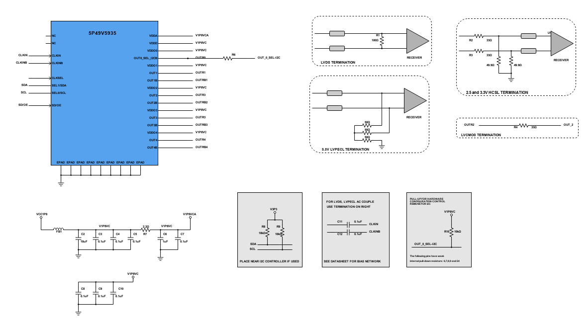
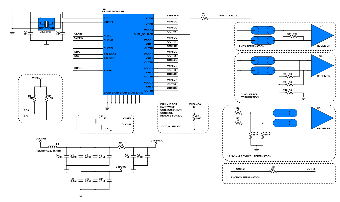
5P49V5935 - VersaClock 5 Programmable Clock Generator with Integrated Crystal
This reference design features the use of 5P49V5935 programmable clock generator that is well suited for networking and data communications applications. It is the fifth generation of programmable clock technology that has an integrated 25MHz crystal as input reference. It allows up to 4 different configurations to be programmed which is accessible using processor GPIOs or bootstrapping. The different selections may be used for different operating modes.
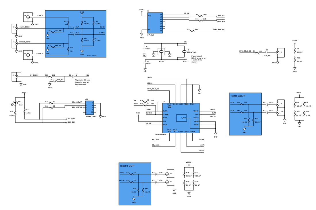
5P49V5943/5944 VersaClock 5 Programmable Clock Generator
The 5P49V5943/5944 fifth generation IDT programmable clock generator is designed to support applications such as networking, industrial, data communications, etc. It can generate up to two independent output frequencies from a single input reference clock. This device has two select pins that allow up to four configurations to be programmed and is accessible using a processor GPIOs or bootstrapping. Its configurations can be stored in on-chip One-Time Programmable (OTP) memory or be changed through its I2C interface.
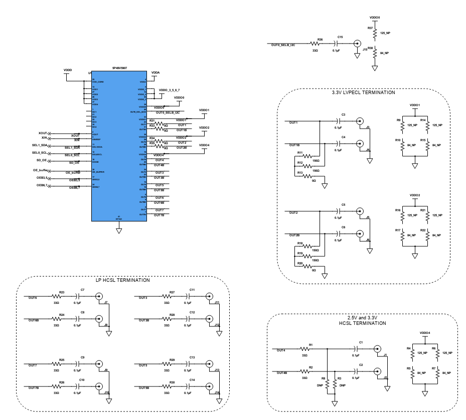
5P49V5907 VersaClock 5 Programmable Clock Generator
The clock generator produces a timing signal (clock signal) for synchronizing a circuit's operation. The VersaClock 5 is ideal for high-performance consumer, networking, industrial, computing, and data-communications applications. This circuit design is the evaluation board for the 5P49V5907 programmable clock generator with RMS phase jitter is less than 0.75 picoseconds over the full 12kHz to 20MHz integration range. The device meets the stringent jitter requirements of PCI Express Gen 1/2/3, USB 3.0, and 1G / 10G Ethernet.
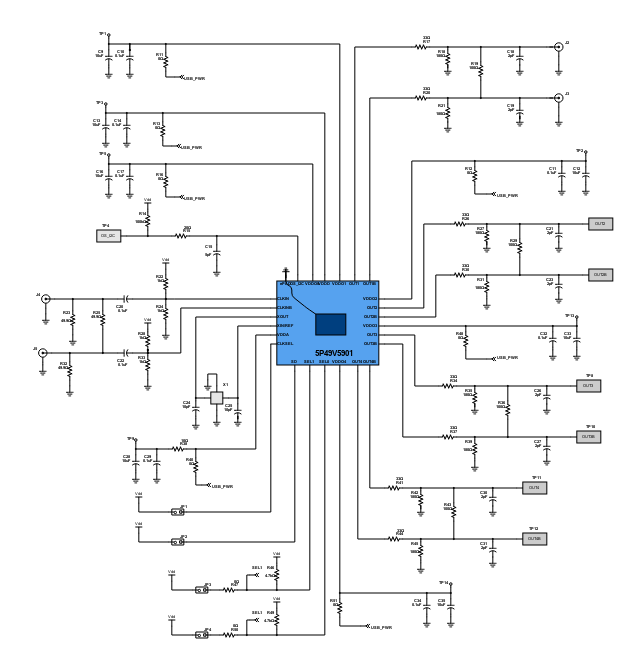
VersaClock 5 - 5P49V5901 Programmer Board
This design features a programmable clock generator which can provides up to four independent output frequencies. The device configuration is stored in an on-chip One-Time-Programmable (OTP) memory which is loaded on startup. The configuration can be modified in operation through I2C interface and the parameters that can be configured include frequency, output signalling and level, loop bandwidth, output to output skew, and crystal load capacitance.The VersaClock 5 typically provides less than 0.7ps RMS phase jitter (integrated from 12kHz - 20 MHz) at the outputs. It is a programmable through I2C serial programming interface. It also features spread spectrum.
Programmable Fanout Buffer
The clock generator produces a timing signal (clock signal) for synchronizing a circuit's operation. The VersaClock 5 is ideal for high-performance consumer, networking, industrial, computing, and data-communications applications. This circuit design is the evaluation board for the 5P49V5907 programmable clock generator with RMS phase jitter is less than 0.75 picoseconds over the full 12kHz to 20MHz integration range. The device meets the stringent jitter requirements of PCI Express Gen 1/2/3, USB 3.0, and 1G / 10G Ethernet.
9FGL0841 - PCI-Express Clock Generator
This clock generator reference design is a 3.3V PCIe Gen1-2-3 Clock Generator. Its main component is the 9FGL0841, a member of IDT's 3.3V low-power PCIe family. The device has eight output enables for clock management and supports 2 different spread spectrum levels in addition to spread off. The output features eight 100MHz Low-Power High Speed Current Steering Logic (LP-HCSL) differential pairs and a 3.3V Low Voltage CMOS (LVCMOS) REF output with Wake-On-LAN (WOL) support.
Introduction
Schematic Drawings
Use schematic symbols to layout the components of your circuit and make electrical connections. With symbols ranging from amplifiers to vacuum tubes, as well as the ability to build custom symbols, you are able to design nearly any circuit. Access to Digi-Key's extensive part database also allows you to browse and assign orderable part numbers.
Diagram Building
Use the system blocks to refine your idea at a conceptual level. The higher-level components are there to help you plan out the broader intentions of your idea. This powerful block chain library allows you to quickly layout the function of circuit. Once your design is ready, save and share with your colleagues.
Flow Chart Creation
The flow chart creation option will help transition your concept to a design. Use the library of arrows, shapes, UML symbols, and more to sort out the flow and annotate each stage. Insert a textbox, math function/formula, image, or link to help illustrate the objectives and make your plan easy to follow.
Help & Resources
Need help? Ask questions in our TechForum

Conversion Calculators
Digi-Key's online conversion calculators offer a one-stop resource for many electronics industry calculations.
Go to Calculators
Conversion Calculators
Digi-Key's online conversion calculators offer a one-stop resource for many electronics industry calculations.
Go to Calculators

Reference Design Library
Search for designs based on the circuit's performance using Digi-Key's Reference Design Library.
Go to Reference Design Library
Reference Design Library
Search for designs based on the circuit's performance using Digi-Key's Reference Design Library.
Go to Reference Design Library
Tech Forum
Feedback
You are about to delete project
Please type 'DELETE' (without quotes) to the below box to confirm the deletion: