Scheme-it
Introduction
Schematic Drawings

Use schematic symbols to layout the components of your circuit and make electrical connections. With symbols ranging from amplifiers to vacuum tubes, as well as the ability to build custom symbols, you are able to design nearly any circuit. Access to Digi-Key's extensive part database also allows you to browse and assign orderable part numbers.
Diagram Building

Use the system blocks to refine your idea at a conceptual level. The higher-level components are there to help you plan out the broader intentions of your idea. This powerful block chain library allows you to quickly layout the function of circuit. Once your design is ready, save and share with your colleagues.
Flow Chart Creation
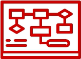
The flow chart creation option will help transition your concept to a design. Use the library of arrows, shapes, UML symbols, and more to sort out the flow and annotate each stage. Insert a textbox, math function/formula, image, or link to help illustrate the objectives and make your plan easy to follow.
Projects
Design Starters help give you a running start for your next design. Whether you are looking to begin a wireless charging platform or quickly design around a Bluetooth Low Energy module, our Design Starters will help get you quickly on your way.
Digi-Key has worked with industry leaders to help drive almost instantaneous ideation and these starters are ideal building blocks to help get your concepts created, drawn and documented in almost no time at all. Featured Design Starters
12 items
Refine Search
APPLICATION
MANUFACTURER
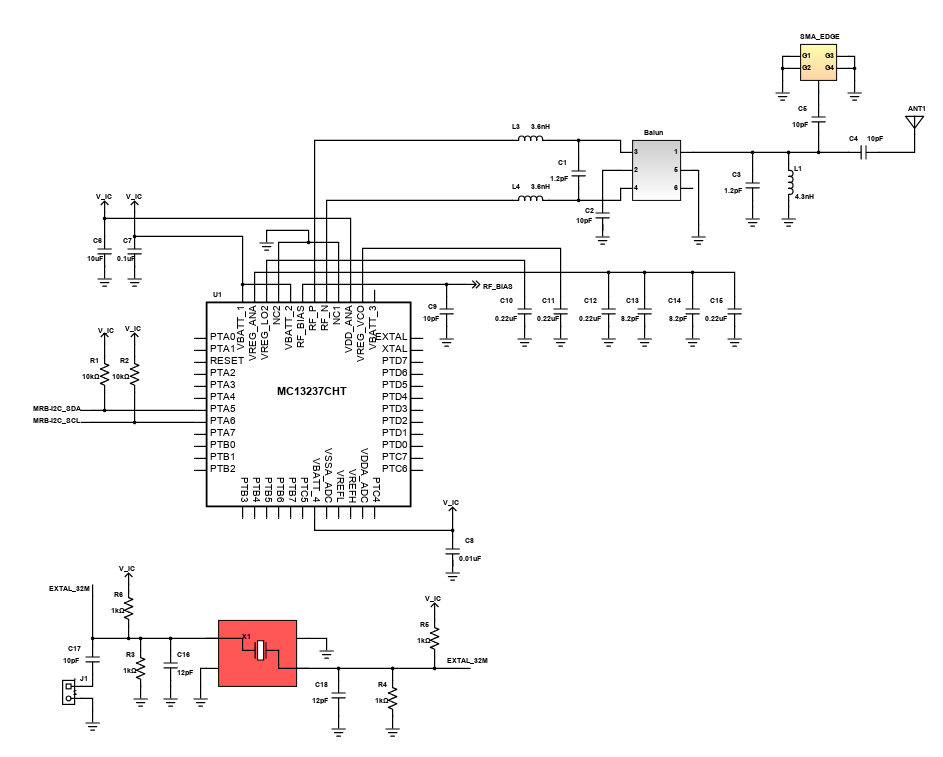
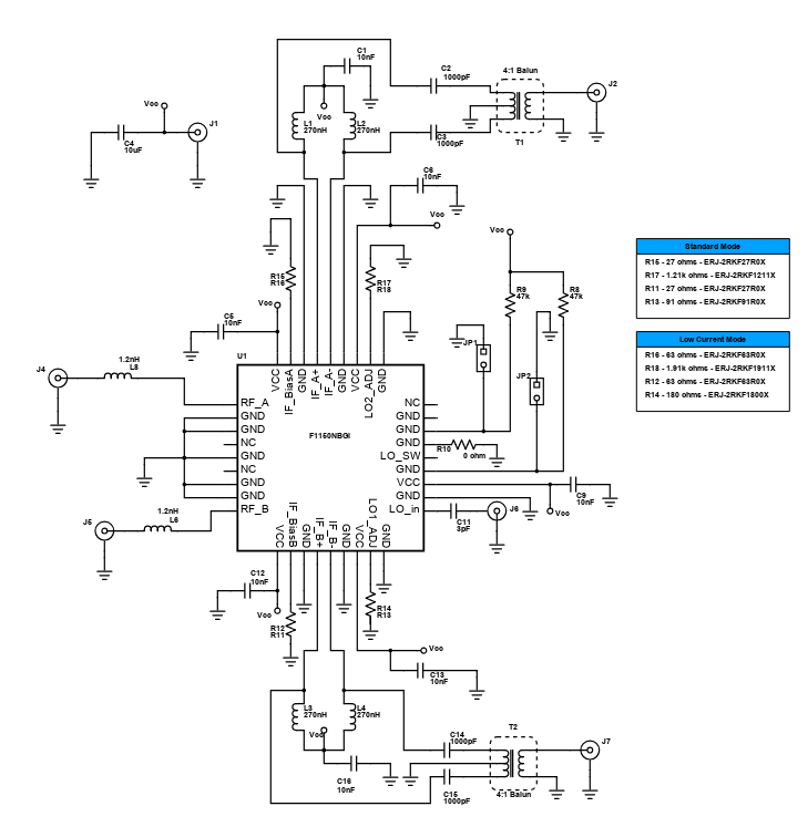
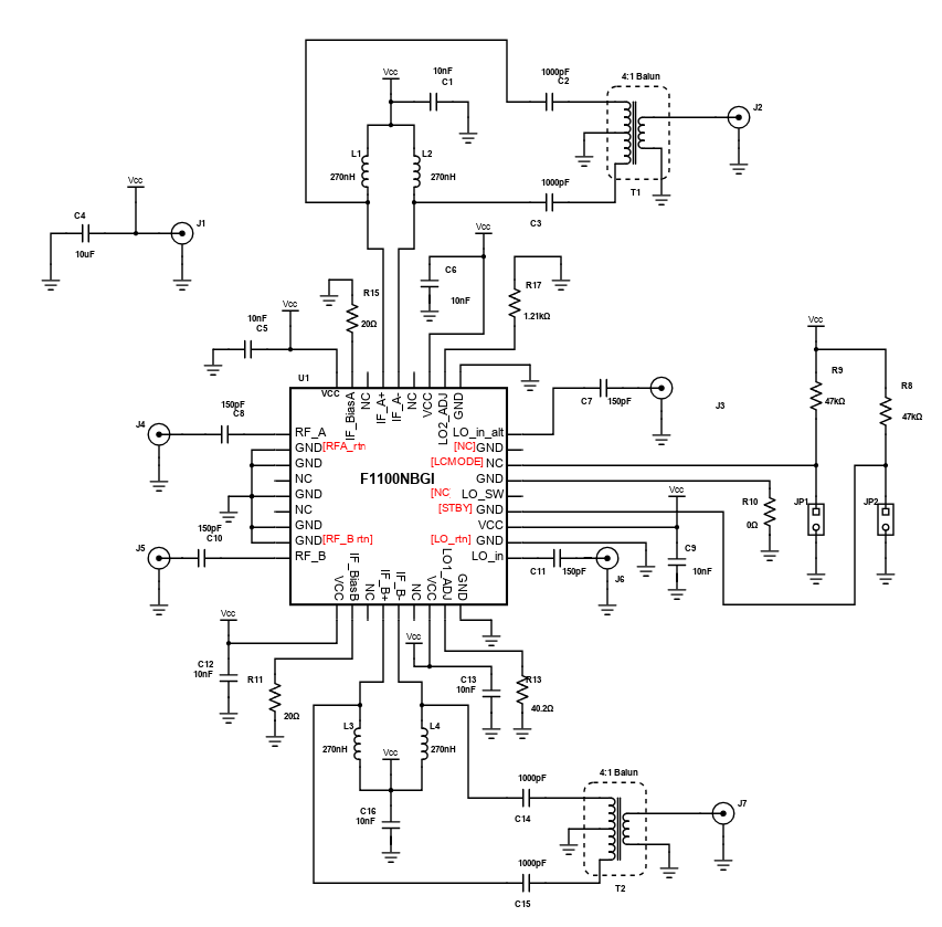
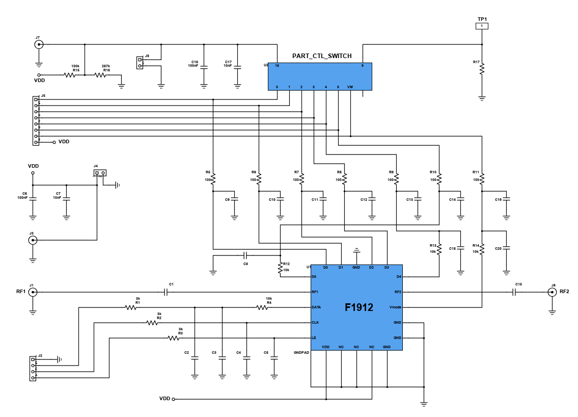
F1150 Dual RF to IF Downconverting Mixer
In RF and microwave applications in communication, a mixer is used to modulate or demodulate a signal. The purpose of using a mixer is to change the frequency of an electromagnetic signal without changing the phase and amplitude of the signal; this allows amplification of the received signal at a frequency other than that of the RF. The IDTF1150 Zero-Distortion RF to IF downconverting mixer is part of a series of downconverting mixers that offers high side or low side injection options for all UTRA (UMTS Terrestrial Radio Access) bands. The F1150 has a UTRA bands of 1,2,3,4,9,10, 33, 34, 35, 36, 37, and 39 with a RF frequency range of 1700 to 2200 MHz, its IF frequency range is 50 - 450 MHz with High Side Injection.
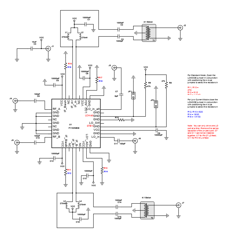
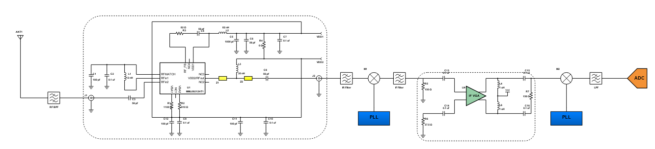
RF to IF Dual Downconverting Mixer
The reference design as shown is a F1100 Zero-Distortion RF to IF Downconverting Mixer. An RF mixer is a 3-port active or passive device that can either modulate or demodulate a signal. These three ports are referred to as the RF input port, LO (local oscillator) input port, and the IF (intermediate frequency) output port. It yields both a sum and difference frequency at a single output port when two distinct input frequencies are inserted into the other two ports. It can be further used as a phase detector or as a demodulator. The two signals inserted into the two input ports are usually the Local Oscillator signal, and the incoming (for a receiver) or outgoing (for a transmitter) signal. A mixer is also known as a downconverter if the mixer is part of a receiver or as an upconverter if it is part of a transmitter.
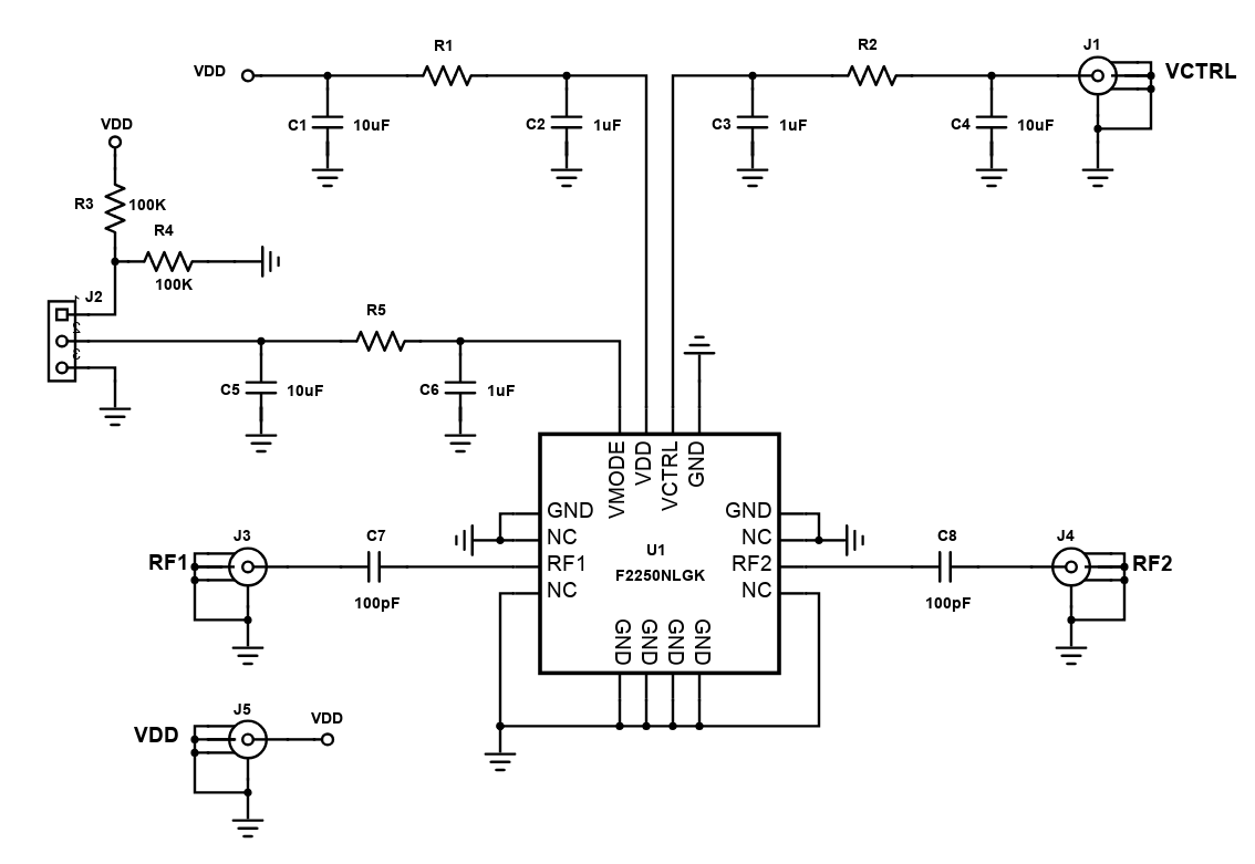
Low Insertion Loss, Voltage-Variable Attenuator Circuit
Attenuators are devices that are used to decrease the amplitude or power of a certain RF signal. These devices are the opposites of amplifiers which increase the power of the signal. A good attenuator is characterized by broad frequency range, low distortion, and has a very minimum loss. Low distortion means fidelity in which in this case, the device retains the original form of the signal even after it has decreased its amplitude. Meanwhile, minimum loss pertains to the efficiency of the device in decreasing the power of the RF signal. These losses include insertion loss and return loss. Insertion loss is the signal power that is lost as a result from insertion from the device to a transmission line or an optical fiber while, return loss is the power lost when the signal is reflected during the transmission.
F1953 - 6-bit 0.50dB Glitch-Free™ Digital Step Attenuator with Internal DC Blocks
This design is a 6-bit glitch-free Digital Step Attenuator (DSA) with internal DC blocks. It has an attenuation error of less than 0.5dB with excellent accuracy. The purpose of attenuation is to protect the circuit from receiving a significant amount of signal and to improve impedance matching. The DSAs are optimized for the demanding requirements of communication infrastructure. It also provides gain control in receivers and transmitters.
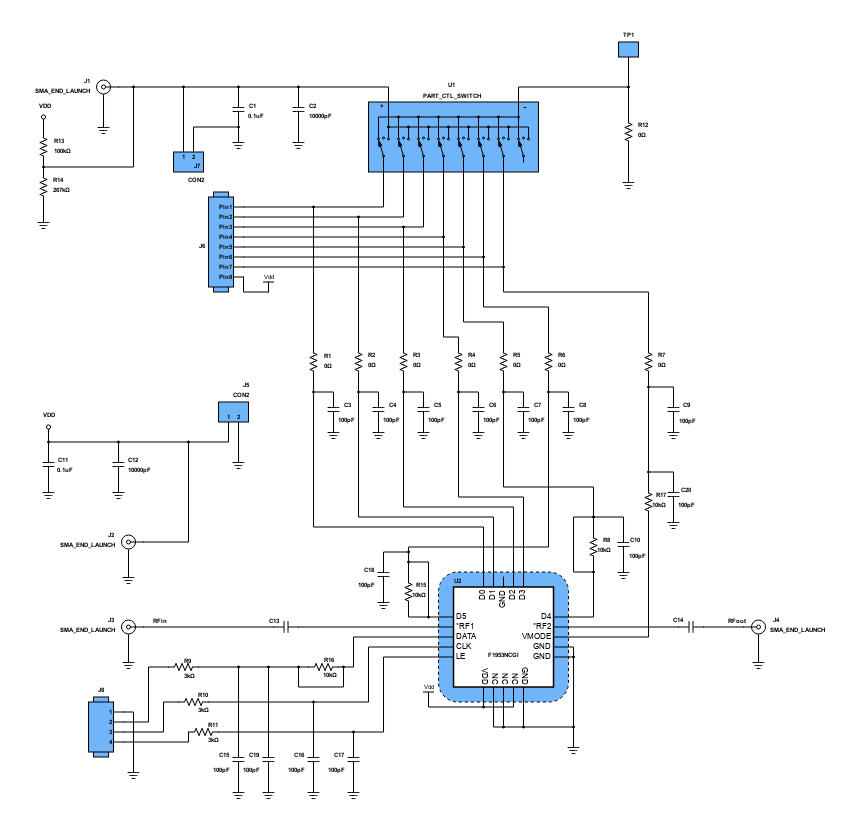
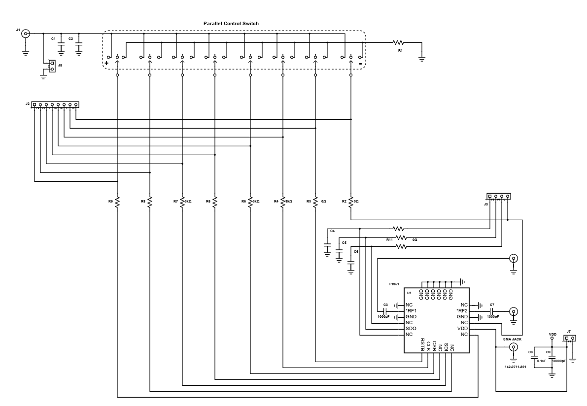
F1951 - 6-bit 0.50 dB Glitch-Free™ Digital Step Attenuator
This reference design features the F1951 Digital-Step-Attenuator (DSA) of IDT with glitch-free technology which effectively improves the system's reliability and settling time. It uses a 6-bit 0.5 dB step attenuator that conforms to the requirement of communications infrastructure. Digital step attenuators are commonly used in receivers and transmitters for gain control. It basically reduces the power of a signal without appreciably distorting its waveform.
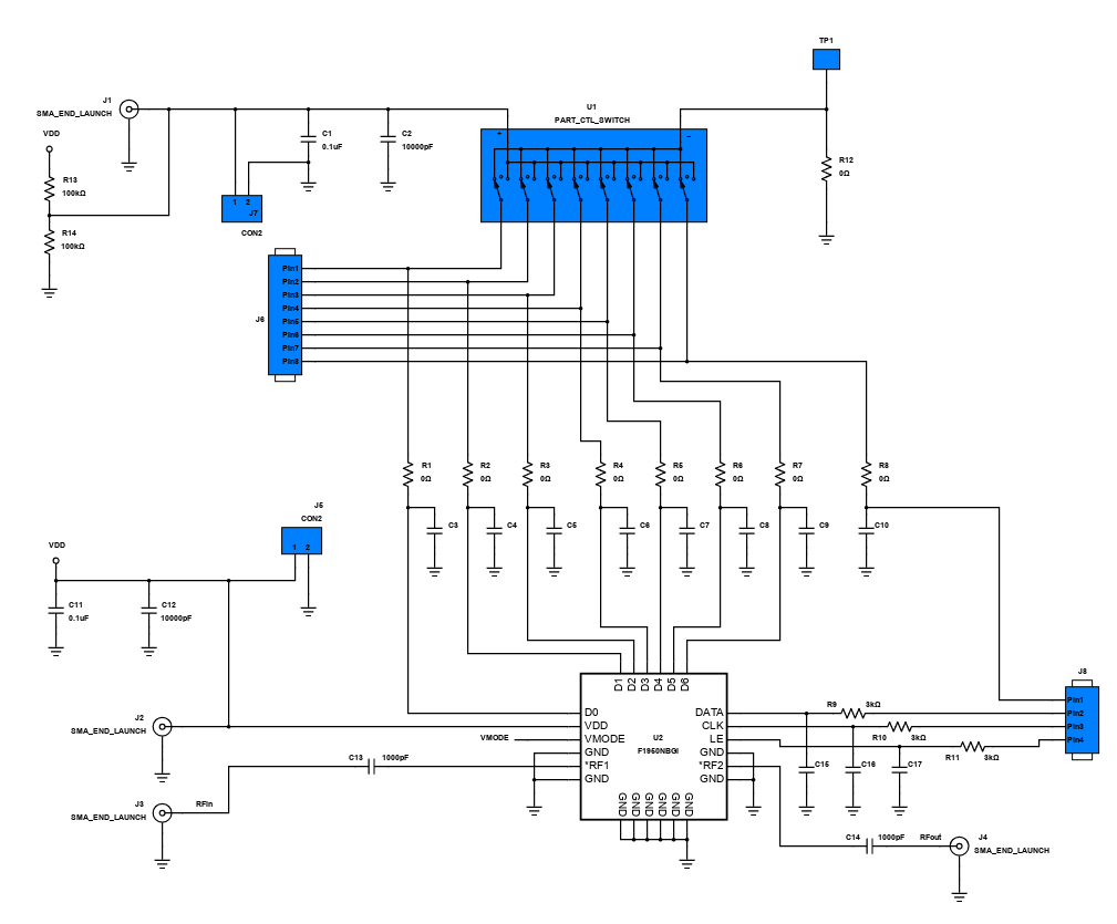
F1950 - 7-bit 0.25 dB Glitch-Free™ Digital Step Attenuator
A digital step attenuator (DSA) is an electronic device used in communication systems, either in a transmitter or a receiver, to provide gain control. This is to protect the circuit that will receive the signal from accepting a signal level that is too high for it to receive. The important characteristics of a radio frequency attenuator are accuracy, low standing wave ratio, repeatability and flat frequency response. It is very important that the waveform of the signal being attenuated must not be changed or distorted by the attenuator.
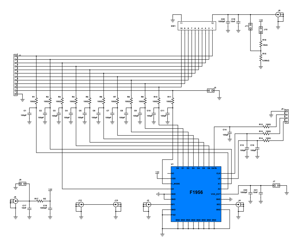
7-bit 0.25dB Glitch-Free Wideband Digital Step Attenuator
This design is a 7-bit glitch-free wideband digital step attenuator with 0.25dB attenuation. An RF Attenuator is the opposite of an RF amplifier in that it reduces the amount of signal power in a system (i.e. attenuates the signal). Attenuation is required when the received signal level is too high that the system could not handle. The purpose of attenuation is to protect the circuit from receiving a significant amount of signal and to improve impedance matching.
6-bit 0.5 dB Glitch-Free™ Wideband Digital Step Attenuator
In RF circuits, an RF attenuator is a device used to reduce the magnitude of a signal without appreciably distorting its waveform. This attenuation is required for protection to circuits that cannot handle high-magnitude signals. An attenuator also provides good impedance matching between two circuit stages and can also be used in a variety of areas where signal levels need to be controlled. The important characteristics of an RF attenuator are high-accuracy, low SWR (Standing Wave Ratio), flat frequency response and repeatability.
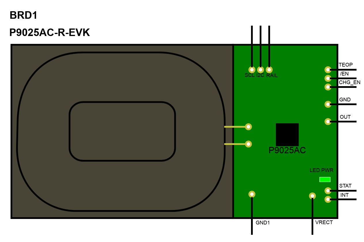
Wireless Power Receiver Symbol
This board is an evaluation for P9025AC wireless power receiver IC from Integrated Device Technology. The P9025AC-R-EVK is a turnkey 5 Watt, Qi-compliant wireless power receiver reference kit for fast prototyping and design integration. The kit consists of an easy-to-use reference board and comprehensive support collateral that significantly eases design-in effort and minimizes time-to-market.This board has the following features and benefits:
• 5.3 V, 1 A output
• WPC 1.1.2 (Qi) compliant for interoperability
• Compact form factor for fast prototyping
• Layout module provided for direct copy to system board
• Optimized PCB reference layout and fully-tested BOM
• Programmable FOD setting via external resistor simplifies tuning process
• Integrated full-bridge synchronous rectifier and LDO for low BOM cost, low manufacturing cost, and small PCB area
Introduction
Schematic Drawings
Use schematic symbols to layout the components of your circuit and make electrical connections. With symbols ranging from amplifiers to vacuum tubes, as well as the ability to build custom symbols, you are able to design nearly any circuit. Access to Digi-Key's extensive part database also allows you to browse and assign orderable part numbers.
Diagram Building
Use the system blocks to refine your idea at a conceptual level. The higher-level components are there to help you plan out the broader intentions of your idea. This powerful block chain library allows you to quickly layout the function of circuit. Once your design is ready, save and share with your colleagues.
Flow Chart Creation
The flow chart creation option will help transition your concept to a design. Use the library of arrows, shapes, UML symbols, and more to sort out the flow and annotate each stage. Insert a textbox, math function/formula, image, or link to help illustrate the objectives and make your plan easy to follow.
Help & Resources
Need help? Ask questions in our TechForum

Conversion Calculators
Digi-Key's online conversion calculators offer a one-stop resource for many electronics industry calculations.
Go to Calculators
Conversion Calculators
Digi-Key's online conversion calculators offer a one-stop resource for many electronics industry calculations.
Go to Calculators

Reference Design Library
Search for designs based on the circuit's performance using Digi-Key's Reference Design Library.
Go to Reference Design Library
Reference Design Library
Search for designs based on the circuit's performance using Digi-Key's Reference Design Library.
Go to Reference Design Library
Tech Forum
Feedback
You are about to delete project
Please type 'DELETE' (without quotes) to the below box to confirm the deletion: