Scheme-it
Introduction
Schematic Drawings

Use schematic symbols to layout the components of your circuit and make electrical connections. With symbols ranging from amplifiers to vacuum tubes, as well as the ability to build custom symbols, you are able to design nearly any circuit. Access to Digi-Key's extensive part database also allows you to browse and assign orderable part numbers.
Diagram Building

Use the system blocks to refine your idea at a conceptual level. The higher-level components are there to help you plan out the broader intentions of your idea. This powerful block chain library allows you to quickly layout the function of circuit. Once your design is ready, save and share with your colleagues.
Flow Chart Creation
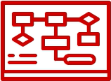
The flow chart creation option will help transition your concept to a design. Use the library of arrows, shapes, UML symbols, and more to sort out the flow and annotate each stage. Insert a textbox, math function/formula, image, or link to help illustrate the objectives and make your plan easy to follow.
Projects
Design Starters help give you a running start for your next design. Whether you are looking to begin a wireless charging platform or quickly design around a Bluetooth Low Energy module, our Design Starters will help get you quickly on your way.
Digi-Key has worked with industry leaders to help drive almost instantaneous ideation and these starters are ideal building blocks to help get your concepts created, drawn and documented in almost no time at all. Featured Design Starters
12 items
Refine Search
APPLICATION
MANUFACTURER
Wireless Power Receiver Schematic
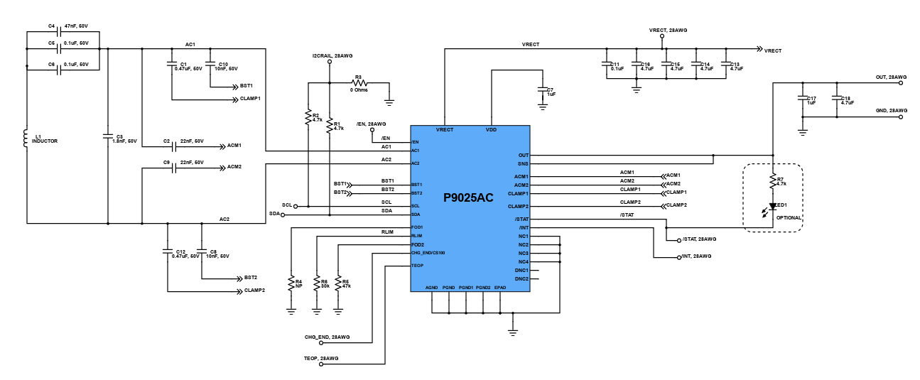
The technological development of power transmission evolves to integrated circuits in which it optimizes the capability of wireless power transfer. This latest design of IDT on wireless application featured a wireless power receiver board with fully integrated single chip solution that requires only few external discrete components . It can support up to 6W output power and WPC V1.1.2 compliant. It has peak efficiency of up to 83%. It make use of an integrated synchronous full bridge rectifier and integrated tracking LDO output stage for its regulation. The system has its own protection against over temperature/current/voltage while a thermal control loop is used to manage the temperature of the system.
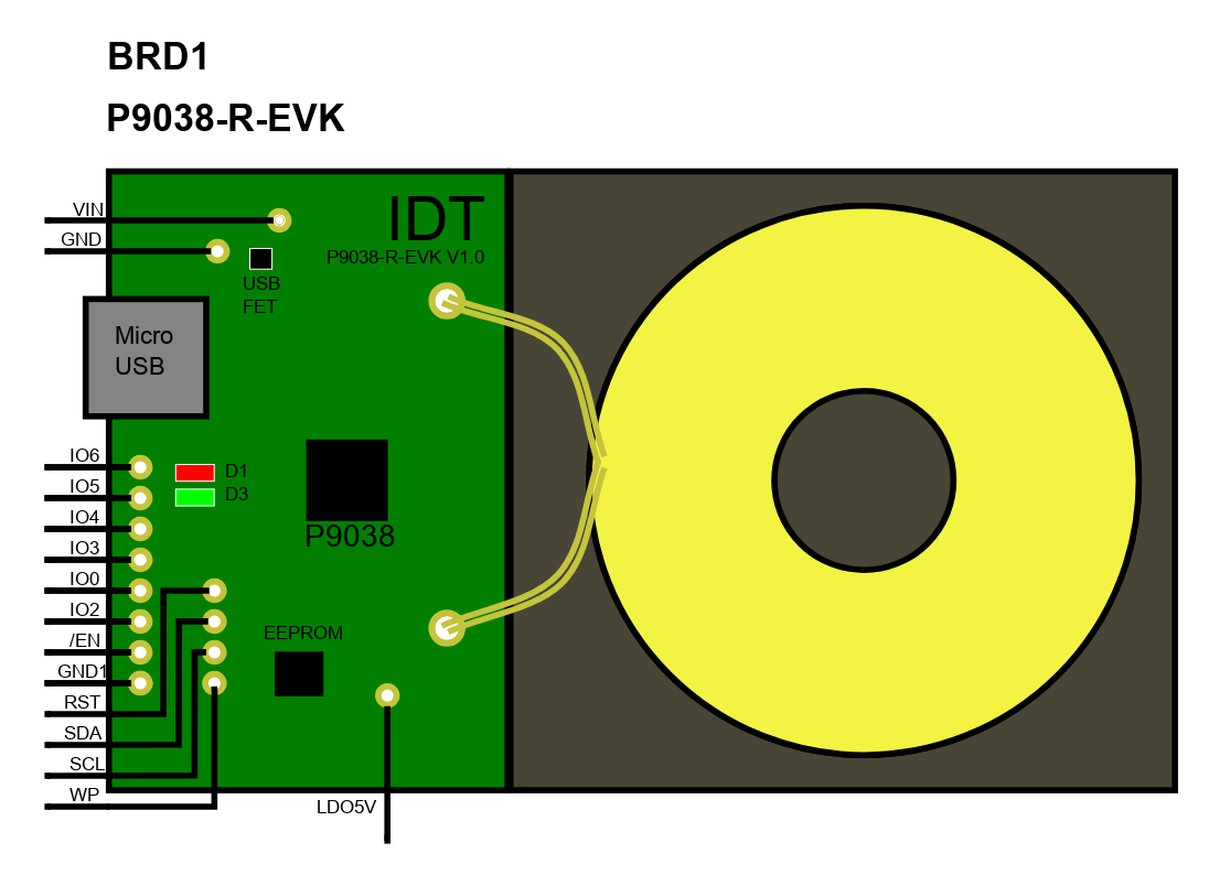
Wireless Power Transmitter Symbol
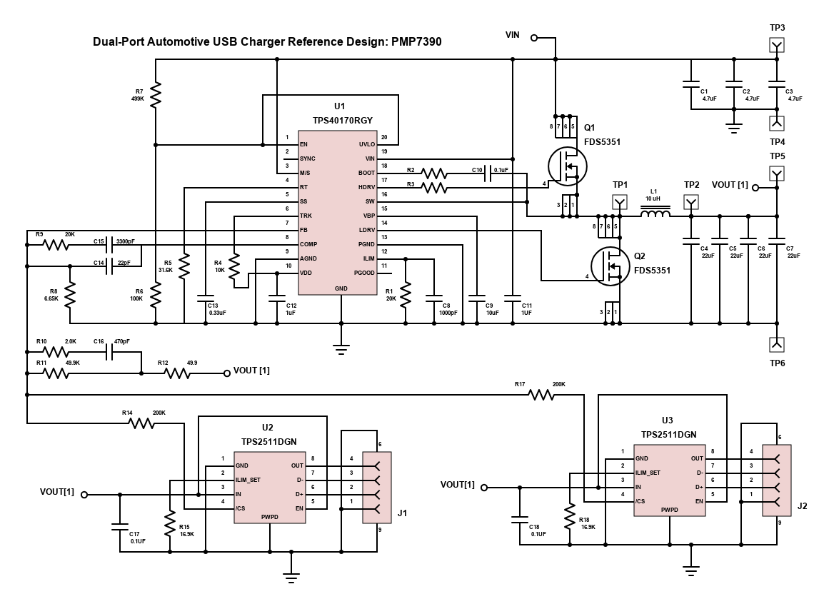
This reference board is a 5W Qi wireless power transmitter from Integrated Device Technology. This circuit evaluation is a 5W, Qi-compliant kit for fast prototyping and design integration. The kit consists of an easy-to-use reference board and comprehensive support collateral that significantly eases design-in effort and minimizes time-to-market.
Here are some features and benefits of this wireless transmitter board:
• WPC 1.1.2 (Qi) compliant for interoperability Compact form factor for fast prototyping
• Layout module provided for direct copy to system board
• 2-layer PCB reference layout and fully-tested BOM
• 4.5 to 6.9 V input, designed for 5 W output on the receiver
• Integrated power stage for low BOM cost, low manufacturing cost, and small PCB area • Input in-rush control prevents surges with inexpensive power adapters
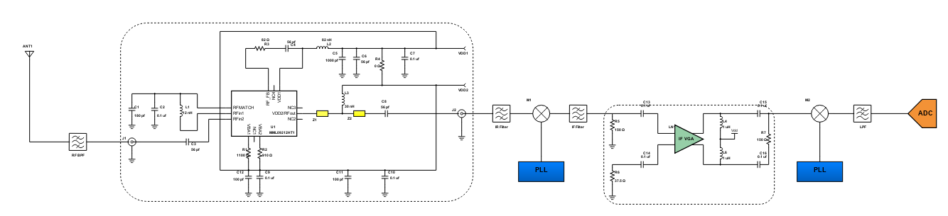
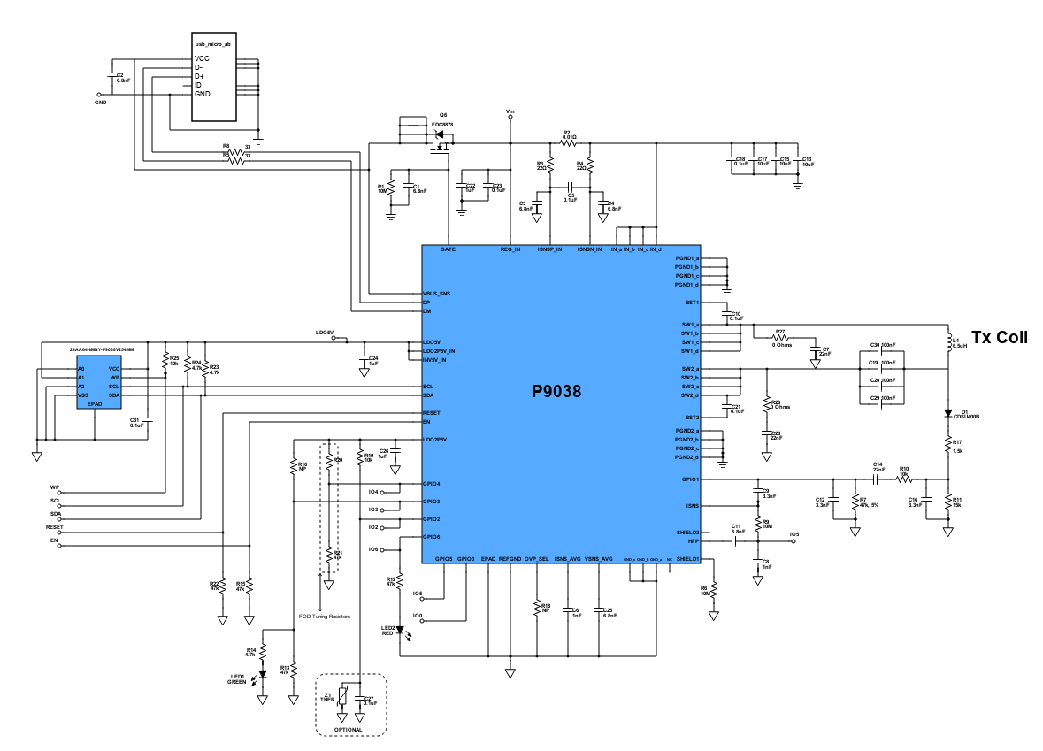
Wireless Power Transmitter Schematic
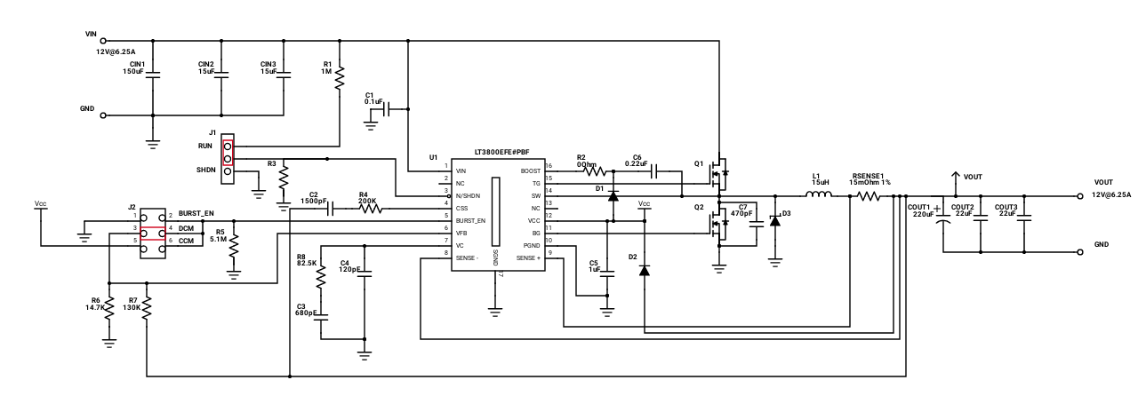
This design features a wireless power transmitter that supports Qi enabled smartphones and other devices. It operates from a 4.5 - 6.9V input and supports up to 8W power transfer at approximately 1.6A. The low cost adaptors and other unregulated adaptors or supplies help prevent surges. Because, it is a fully integrated design, BOM cost is minimal while still offering highly efficient operations with very low RDS(ON). It also has programmable input in-rush control that can be used to add up protections and configurations of the system.
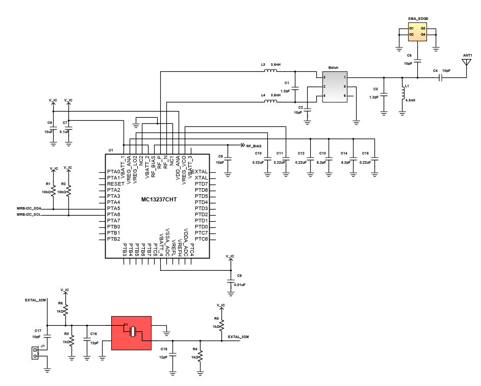
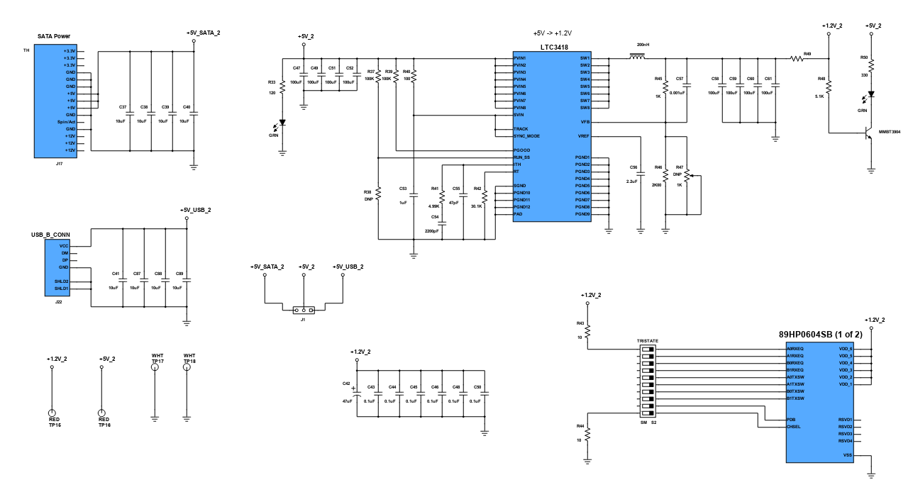
SAS/SATA Signal Repeater
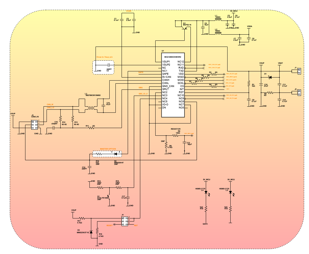
The Serial Attached SCSI (SAS) and Serial AT Attachment (SATA) technology both provides high-speed data transfer rate. Using the SATA III (revision 3.x) interface, data can travel up to 6Gbps. But just like in any communication links, the signal travelling across SAS/SATA interface degrades as the trace and cable lengths within a computer, a storage or a communication system gets longer. Hence, redrivers/repeaters recondition the signal so that system receiver can get a reliable data.
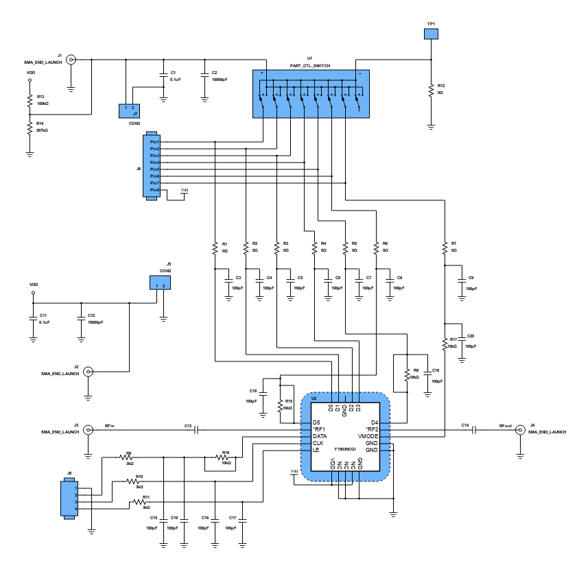
PCI-E Signal Repeater
This reference design introduces the use of signal repeaters of IDT that effectively maintain signal integrity in the system. Basically, when an information-bearing signal passes through a communication channel, it is progressively degraded due to loss of power. However, with this PCI-E signal repeater, signals are conditioned and boosted. Thus, delivering signal quality while offering simplified design.
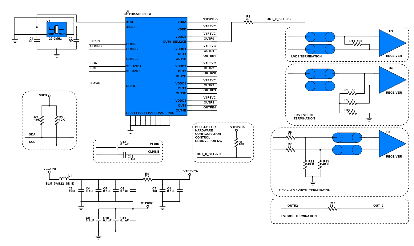
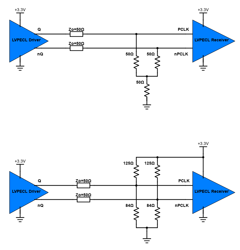
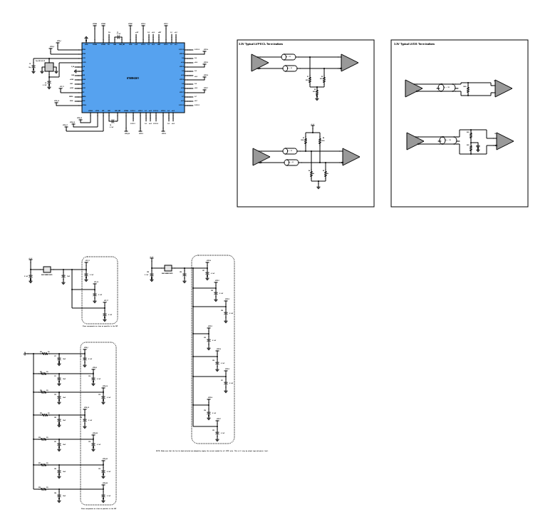
Typical LVPECL Output Termination
Low voltage positive emitter coupled logic (LVPECL) is an established high frequency differential signaling standard. It is an enhanced version of Positive emitter coupled logic (PECL), a differential signaling systems that is usually used in high speed and clock distribution circuits. The ICS853S01I is a high performance Differential to LVPECL Multiplexer. It can also perform differential translation because the differential inputs accept LVPECL, LVDS and CML levels. The ICS853S01I is packaged in a small 3mm x 3mm 16 VFQFN package, making it ideal for use on space-constrained boards.
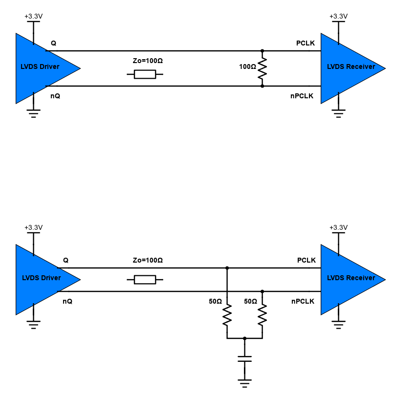
Typical LVDS Output Termination
The Low-Voltage Differential Signaling (LVDS) is a communication standard; it can operate at a low power at a very high speed on a twisted pair copper cable. LVDS operates in both parallel and serial data transmission. In parallel transmissions multiple data differential pairs carry several signals at once including a clock signal to synchronize the data. In serial communications, multiple single-ended signals are serialized into a single differential pair with a data rate equal to that of all the combined single-ended channels.
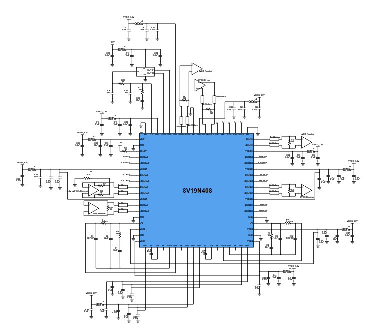
8V19N408 FemtoClock NG Jitter Attenuator and Clock Synthesizer
The 8V19N408 is part of the family of fully integrated FemtoClock NG jitter attenuators and clock synthesizer. It has two stages of PLL (Phase Lock Loop) the same with 8V19N407, the stage 2 PLL compared to the 8V19N407 that has two choices for the VCO of the stage 2 PLL but has only a single VCO for the target frequency synthesis. The 8V19408 is more flexible for it has a dual internal VCO in the stage 2 PLL and either one can be selected; the first VCO frequency at 2400-2500MHz and the second VCO frequency at 2920 - 3000MHz. It has five differential clock outputs configurable as LVPECL or LVDS variable output amplitude. Four differential system reference (SYSREF) signal outputs for JESD204B and can also be used as additional clock outputs.
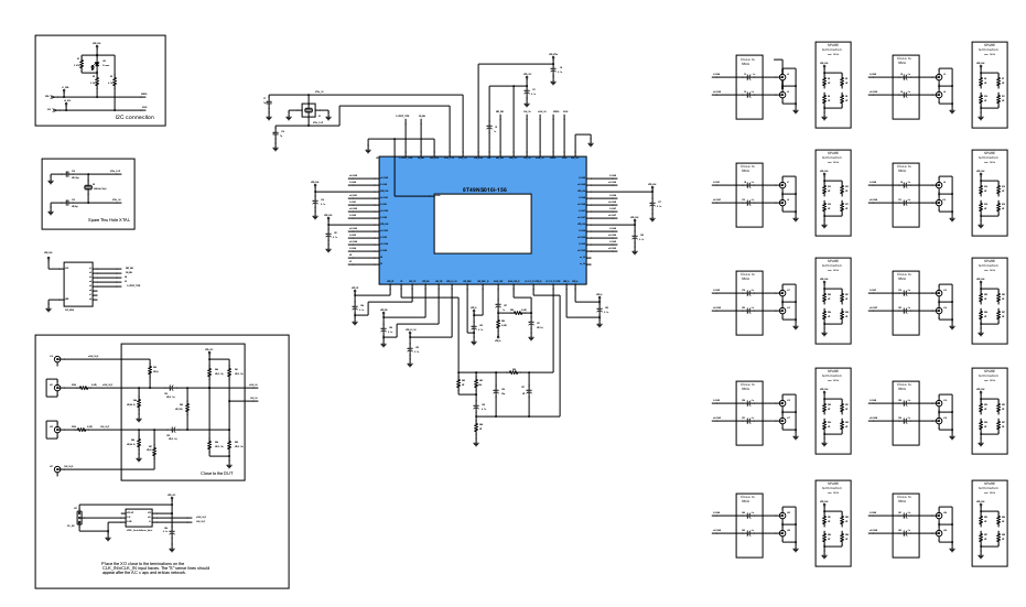
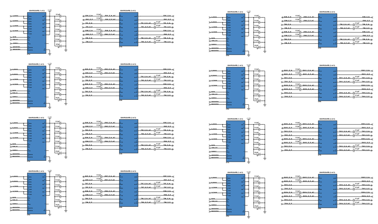
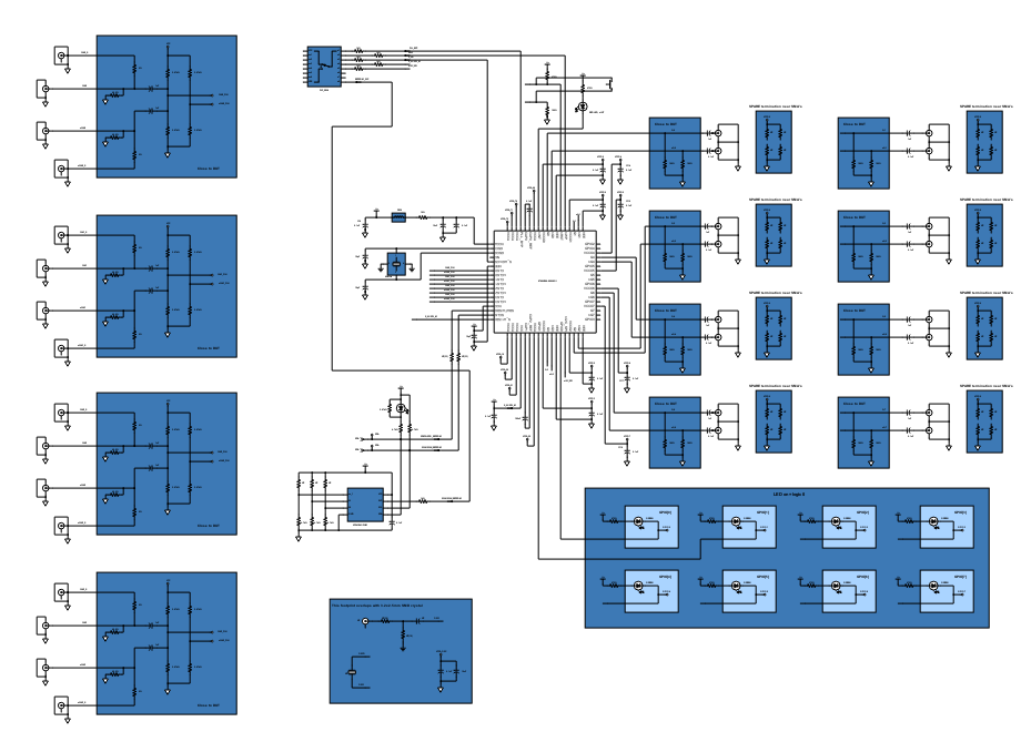
8T49N286 RevA Evolution Board Schematic
This evaluation board allows the designer of data communication equipment to know the general idea about the product. It also enables the designers to evaluate the main chip "8T49N286" with eight LVPECL outputs capable of generating any output frequency using IDT Timing Commander Software. It also comes with SMA connectors for each output pair while the output termination requires 50Ω resistance.
8T49N281 Universal Frequency Translator
This reference design is a universal frequency translator of IDT that uses 8T49N281 clock generator. This IC has a fractional-feedback PLL that can be used as a jitter attenuator or frequency translator. It is equipped with six integer and two fractional output dividers, allowing the generation of up to 8 different output frequencies, ranging from 8kHz to 1GHz. The eight outputs may select among LVPECL, LVDS or LVCMOS output levels.
Introduction
Schematic Drawings
Use schematic symbols to layout the components of your circuit and make electrical connections. With symbols ranging from amplifiers to vacuum tubes, as well as the ability to build custom symbols, you are able to design nearly any circuit. Access to Digi-Key's extensive part database also allows you to browse and assign orderable part numbers.
Diagram Building
Use the system blocks to refine your idea at a conceptual level. The higher-level components are there to help you plan out the broader intentions of your idea. This powerful block chain library allows you to quickly layout the function of circuit. Once your design is ready, save and share with your colleagues.
Flow Chart Creation
The flow chart creation option will help transition your concept to a design. Use the library of arrows, shapes, UML symbols, and more to sort out the flow and annotate each stage. Insert a textbox, math function/formula, image, or link to help illustrate the objectives and make your plan easy to follow.
Help & Resources
Need help? Ask questions in our TechForum

Conversion Calculators
Digi-Key's online conversion calculators offer a one-stop resource for many electronics industry calculations.
Go to Calculators
Conversion Calculators
Digi-Key's online conversion calculators offer a one-stop resource for many electronics industry calculations.
Go to Calculators

Reference Design Library
Search for designs based on the circuit's performance using Digi-Key's Reference Design Library.
Go to Reference Design Library
Reference Design Library
Search for designs based on the circuit's performance using Digi-Key's Reference Design Library.
Go to Reference Design Library
Tech Forum
Feedback
You are about to delete project
Please type 'DELETE' (without quotes) to the below box to confirm the deletion: